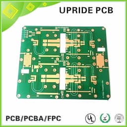
Enig Charger Printed Pcbs Circuit Board
- Estimate pricingPrice on request
- Base MaterialFR4, CEM-1, Aluminium, High Tg Material, Halogen-free Material
- Layer Count1-12 Layers
- Board Thickness0.2-3.0 mm
- Min. Hole Diameter (Mechanical)0.15 mm
Your request goes to Ke You Pcb Co., Ltd. Follow up with them in Messages on Global Trade Plaza.
Products Description
We OffeCircuit Boardr a Full Range of Printed Circuit Board Capabilities to Fit All of Your PCB Needs Process Item Craft Capacity Prepares materials Base Material FR4, CEM-1, Aluminium, High Tg Material, Halogen-free Material Lamination press Layer Count 1-12Layers Thickness 0.2-3.0mm Drill Min.Hole Diameter 0.15mm (mechanical drill), 0.1MM (laser drill) PTH Diameter Tolerance + / - 3mil NPTH Diameter Tolerance + / - 2mil Outer layer Min.Line/Space 3.5mil/3.5mil Copper Thickness 1- 6oz Impendence Impedance tolerance ±10% (±5%(Need assessment) Solder Masking Min.Solder Dam 0.1mm Min.Solder Mask Opening 0.075mm Color Green, White, Red, Yellow, Black, Blue Surface Treatment LF-HASL, OSP,Ni/Au Enig,Immersion Tin, Immersion Silver, carbon oil; Out-Line Profiling Profile Tolerance + / - 0.12MM V-cut Remain Thickness Tolerance + / - 0.1MM V-cut Angle Tolerance + / - 5° Testing E-Testing 100% E-Testing (High Voltage Testing); Flying Probe Testing Final Product Thickness Tolerance + / - 10% Warpage Tolerance + / - 0.75% Lead Time Double layer PCB Multilayer PCB Mass production Normal 6 work days Normal 8 work days Double layer 9-12 work days Urgent 3 work days Urgent 6 work days Multilayer 12-15 work days Email:sales5@(keyoupcb.com) Learn more from our website:www.keyoucircuit.com ADD:Room K221,jinhetian Center,QINGHU AREA,SHENZHEN, Guangdong,China
Product Categories
Products Specification
- Base MaterialFR4, CEM-1, Aluminium, High Tg Material, Halogen-free Material
- Layer Count1-12 Layers
- Board Thickness0.2-3.0 mm
- Min. Hole Diameter (Mechanical)0.15 mm
- Min. Hole Diameter (Laser)0.1 mm
- Outer Layer Min. Line/Space3.5 mil / 3.5 mil
- Copper Thickness1-6 oz
- Min. Solder Dam0.1 mm
- Min. Solder Mask Opening0.075 mm
- Solder Mask ColorsGreen, White, Red, Yellow, Black, Blue
- Surface TreatmentLF-HASL, OSP, Ni/Au ENIG, Immersion Tin, Immersion Silver, Carbon Oil
- Profile Tolerance±0.12 mm
- V-cut Remain Thickness Tolerance±0.1 mm
- V-cut Angle Tolerance±5°
- Testing100% E-Testing, Flying Probe Testing
- Thickness Tolerance±10%
- Warpage Tolerance±0.75%
- Lead Time (Double Layer, Normal)6 work days
- Lead Time (Double Layer, Mass Production)9-12 work days
- Lead Time (Double Layer, Urgent)3 work days
- Lead Time (Multilayer, Normal)8 work days
- Lead Time (Multilayer, Mass Production)12-15 work days
- Lead Time (Multilayer, Urgent)6 work days



Get a quote from Ke You Pcb Co., Ltd
Enig Charger Printed Pcbs Circuit Board from other sellers



More Enig Charger Printed Pcbs Circuit Board from Category


Post your requirement – Global Trade Plaza
Describe what you need once. Suppliers who deal in it see your requirement as a buy lead and can send you offers.
More related Products from Seller

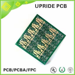


Buy Online Wholesale Enig Charger Printed Pcbs Circuit Board from Supplier & Exporter in
This printed circuit board is offered with a range of fabrication capabilities. Base materials include FR4, CEM-1, aluminium, high Tg and halogen-free laminates, with layer counts from 1 to 12 and board thickness from 0.2 mm to 3.0 mm. Minimum mechanical drill hole diameter is 0.15 mm and laser drill is 0.1 mm, while outer-layer line and space can reach 3.5 mil. Copper thickness options run from 1 oz to 6 oz. Solder mask dams down to 0.1 mm and openings to 0.075 mm are available in multiple colours. Outline profiling tolerance is ±0.12 mm, V-cut remainder thickness tolerance ±0.1 mm and angle tolerance ±5°. Every board undergoes 100% electrical testing, with flying probe testing also offered. Lead times are listed for two categories: normal production (6 work days for double-layer, 8 work days for multilayer) and mass production (9–12 work days for double-layer, 12–15 work days for multilayer), with urgent options of 3 work days for double-layer and 6 work days for multilayer.
Import Wholesale Enig Charger Printed Pcbs Circuit Board for Your Business Needs
The seller has not added a specification yet; ask for the data sheet or test certificate. Ask Ke You Pcb Co., Ltd for a firm quote and delivery terms before you order.
About Supplier
Ke You Pcb Co., Ltd is a B2B supplier based in China, listed on Global Trade Plaza since October 2026. Use Inquire now or Chat with supplier to ask Ke You Pcb Co., Ltd for prices, specifications and documents for Enig Charger Printed Pcbs Circuit Board.
Supplier Details for Enig Charger Printed Pcbs Circuit Board
- Member since - Oct 2026
- Business Type - Contact Seller
- Deals in Product Type - PCB
- Country - China
Frequently Asked Questions (FAQs) on Enig Charger Printed Pcbs Circuit Board
1. What is the Seller’s Policy on Payment for Enig Charger Printed Pcbs Circuit Board?
Ask Ke You Pcb Co., Ltd which payment terms they accept for Enig Charger Printed Pcbs Circuit Board. Agree the payment terms in writing with the supplier before you pay.
2. How to Place an Order for Enig Charger Printed Pcbs Circuit Board with Ke You Pcb Co., Ltd?
Click Get a quote to send your requirement to the supplier Use Chat with supplier to ask questions Post your requirement to hear from other suppliers too
Placing an order for Enig Charger Printed Pcbs Circuit Board with Ke You Pcb Co., Ltd is quick and straightforward on Global Trade Plaza, a leading B2B marketplace for global buyers and suppliers. You can:
3. What Should You Consider When Buying Enig Charger Printed Pcbs Circuit Board Online in 2025?
Product specifications (material, durability, features) Quality certifications and compliance Supplier credibility and customer reviews Minimum Order Quantity (MOQ) and bulk pricing Lead time and delivery timelines
When purchasing Enig Charger Printed Pcbs Circuit Board from a B2B marketplace in 2025, focus on the following critical factors:
Comparing prices and communicating directly with Ke You Pcb Co., Ltd can help ensure value for money and better sourcing decisions.
4. Who Are the Top B2B Importers and Buyers of Enig Charger Printed Pcbs Circuit Board on Global Trade Plaza?
Visit the Buy Leads section Filter by industry, product type, or country Create an account to access full buyer contact details
Global Trade Plaza is home to B2B buyers, wholesalers, distributors, and importers of Enig Charger Printed Pcbs Circuit Board across industries and countries. To discover the most active and high-value buyers:
5. What is the Port of Dispatch, Estimated Price, and Packaging Type Offered by Ke You Pcb Co., Ltd?
Ke You Pcb Co., Ltd, a B2B supplier from China, dispatches Enig Charger Printed Pcbs Circuit Board primarily through the port at China. Packaging types (e.g., bulk, custom, eco-friendly) and estimated pricing may vary based on order volume and destination. To get detailed logistics and pricing information, use Get a quote or Chat with supplier, or Sign Up for direct supplier interaction.





Explore Top Product Categories
- Alcohol Based Hand Sanitizer
- Paper Soap
- Antibacterial Hand Wash
- Cosmetic Kits
- Detergent Chemicals
- Industrial Chemicals
- Laboratory Chemicals
- Leather Chemicals
- Car Accessories
- Motorcycle Parts
- Automobile Brakes Spare Parts
- Motorcycle, Scooters & ATV Bikes
- Building Construction Machineries & Equipments
- Bricks
- Cupboards, Door, Gates, Grills & Windows
- Wall Tiles
- Filters, Water Treatment Plants
- Household Cleaning Products
- Wiping Rags, Mops, Dusters, Sponge, Brushes, Scourer
- Soap & Detergent
- Industrial Gears & Gear Boxes
- Machined Components
- Bolts
- Nuts
- Food Packaging Bags
- Wooden Packaging Boxes
- Offset Printing Machinery & Equipments
- Packaging Machinery
Related Products
Uric Acid Meter Pcba China ManufacturerRigid-flex Printed Pcb Circuit BoardDouble Side Rigid Pcb Circuit Prototype BoardPcba Assembly Made In ChinaIntegrated circuitsTRONCO Electronic Access Control SystemR2R Flexible Printed Circuit AssemblyH61 & H81 Chipsets AvailablePcbPcb Pc Pre-Cure DryerPcb-Ov Pre-Cure DryerPcb-Cz Pre-Cure Dryer33KV Oil Cooled Current TransformerCNC Machining Center Spindles - MV0910Turning Center Spindles - KTG2204CNC External Grinding Spindles - GH1002Tapping Center Spindles - KD0812BBelt Drive Spindle - Horizontal - KT1406Built-in Motor Spindles - PSB0912Used Yamaha 25 HP 4-Stroke Outboard Motor EngineUsed Yamaha 9.9 HP 4-Stroke Outboard Motor EngineUsed Yamaha 50HP 4-Stroke Outboard Motor EngineUsed Yamaha 60HP 4-Stroke Outboard Motor EngineELECTRIC INSULATION GLASS FIBER WOVEN TAPESNectars, juice drinks, soft drink Peach, Apple, Orange, MultifruitBerry juices, soft drink - Berry mix, Strawberries, Raspberries, Cherry, Strawberry-lingonberry, Cranberry, LingonberryGus Smt Pcb Assembly Line G-l120w
Related Categories
PCBATM - Automated Teller MachinesAmplifiersAudio & Video Broadcasting EquipmentsAudio Amplifier & MixerAudio Cassette PartsBanking EquipmentsBluetooth & Related ItemsCD PlayersCDs & CassettesCDs & DVDs CasesCalculatorsCaller ID TelephonesCamcorderColored Picture TubesCommunication DevicesConferencing SystemsCordless PhonesDVD & Blue Ray PlayersDVD & Blue-Ray DiscsDigital Camera & Video CameraDigital DiariesDiodesEarphones & HeadphoneElectronic ActuatorsElectronic AntennaElectronic Audio Goods & Equipment